Quality, test procedures and traceability
Our services
- Automated Optical Inspection, AOI
- Flying-Probe-Test / FPT
- Function test / FT
- In-Circuit-Test / ICT
- thermal imaging
- infrared thermography / IRT
- Solder Paste Inspection - Sinter Paste Inspection / SPI - 3D-SPI
- Manual visual inspection / MVI
- Visual inspection
- X-ray inspection
- X-ray testing
- Mechanical wearing tests
- Mechanical endurance tests
- Random samples
- Periodic samples
- routine tests
- Traceability
Quality decides - decide with us: for quality from AMS
AMS lives quality in the finished products as well as in all steps on the way there.
We are certified according to ISO 9001 and produce on the basis of IPC 610, for further information please see //certifications and memberships
The best proof of quality are our satisfied customers. Many of them have been with us for years. We grant you a small insight under //Our customers
In development and design, quality begins with the requirements analysis - and extends from the conception, a fully functional prototype to the finished serial model. In case of doubt, we go through the individual development steps together with our customers in several iterations - until the result is really perfect!
In production, quality begins with the selection of high-quality components, the use of modern production equipment and skilled personnel with a good eye for detail. This is how we manufacture with high precision - and a low reject rate.
The final quality assurance is the conclusion of the production process. To ensure that everything is always right in the end, we use a variety of different test procedures and test strategies.
The following test procedures are used by us:
Manual visual inspection/ visual inspection (MVI):
Within the scope of manual visual inspection (MVI), the assembled printed circuit boards are visually inspected manually by our long-standing specialists from quality assurance using microscopes. Our many years of experience ensure that even minor deviations are reliably detected. Depending on the requirements, superficial to demanding optical inspections are possible.
The test procedure of visual inspection can be a preferred test method, especially in connection with small quantities and in the context of safety-relevant applications.
Automated Optical Inspection (AOI):
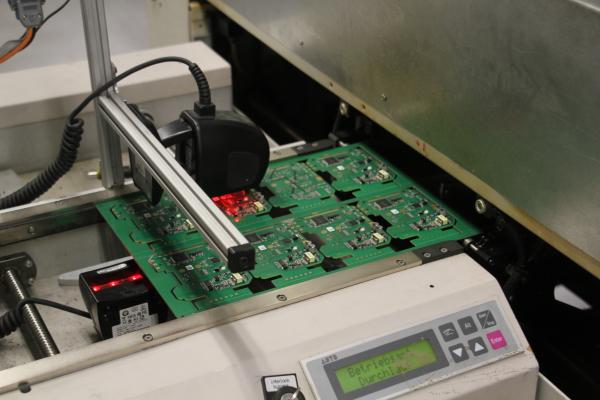
Within the scope of automated optical inspection (AOI), the assembled printed circuit boards are checked for defects by machine using image processing methods. This enables us to reliably identify missing or incorrectly assembled components, twisted or offset components, components that are not or incorrectly soldered, PCB contamination, components that are short-circuited with each other and much more. The automatic optical inspection is a cost-effective way of checking assembled PCBs for possible manufacturing defects quickly, reliably and in large quantities.
Solder paste inspection and sinter paste inspection (SPI/ 3D-SPI):
By means of solder paste inspection and sintering paste inspection, we inspect printed circuit boards after solder paste printing / sintering paste printing with regard to various measurement criteria. This ensures that inadequately soldered or sintered circuit boards can be sorted out at an early stage. Depending on the process and application, different criteria such as shape, height and area, volume, bridges, X/Y offset, coplanarity, particles, notches, holes and fraying are inspected and defects are reliably detected.
Thermal imaging / infrared thermography (IRT):
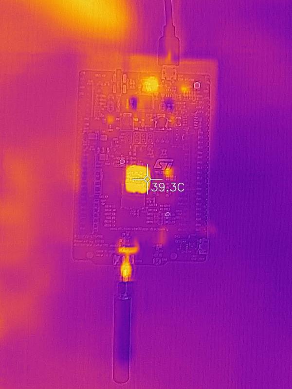
By means of thermal imaging / infrared thermography (IRT), we already detect hotspots and atypical temperature distributions in the development of electronics, which could lead to thermal stress and premature aging and possible failure of individual components. For this purpose we inspect printed circuit board prototypes and in particular integrated circuits (IC's), microcontrollers and multichip modules. We reliably detect soldering defects (e.g. cold solder joints), components that are short-circuited with each other, increased contact resistance (e.g. due to constrictions of conductors), power loss caused by RF mismatch, cracks in joints that cannot be optically detected by masking, verify the correct thermal connection of heat sinks and much more.
In-Circuit Test (ICT)
By means of in-circuit tests (ICT) we check electronic assemblies, circuits and assembled circuit boards with regard to electrical connections and defined component parameters.
For this purpose we insert them into special test adapters, which we also develop and manufacture ourselves according to the respective requirements.
In-Circuit-Tests (ICT's) enable the accurate detection of errors in the conductor path (e.g. short circuits / interruptions), faulty solder joints, component defects and more.
Analog components can be tested or measured along different parameters (e.g. resistance, capacitance, inductance etc.) as well as digital components taking into account previously defined test signals. In each case the effects are detected and compared with the defined target values or the expected effects.
In the context of ICT's, different measuring methods (two-wire measurements, four-wire measurements) are used.
Because of the relatively complex adaptation (due to the development of individual test adapters required as a result) ICT's are mainly used in the context of larger production batches.
Flying Probe Test (FPT)
Flying Probe Tests (FPT's) are a test procedure that is similar in some respects to the In-Circuit Test procedure, but with some differences and specific advantages and disadvantages compared to ICT.
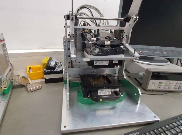
Compared to ICT, FPT uses only a few test needles (usually four on the top and two on the bottom). These are fully automatically driven and contacted to the corresponding test points/measurement points on the assembled PCB (solder pads, pins or test pads), whereby tests on both sides are possible. In this way - analogous to the ICT process - connection errors can be reliably detected.
In contrast to the ICT process, however, the tests of the assembled circuit boards of a panel are not carried out in parallel but sequentially in the FPT process. The test points are touched and tested board by board, which leads to longer test times compared to the ICT method. On the other hand, this procedure leads to greater flexibility in setting up the test projects with regard to changing layouts. In addition, the costs for the development of specific test adapters are eliminated and, compared to the ICT procedure, smaller grid dimensions can be contacted.
X-ray inspection/ X-ray testing (XI):
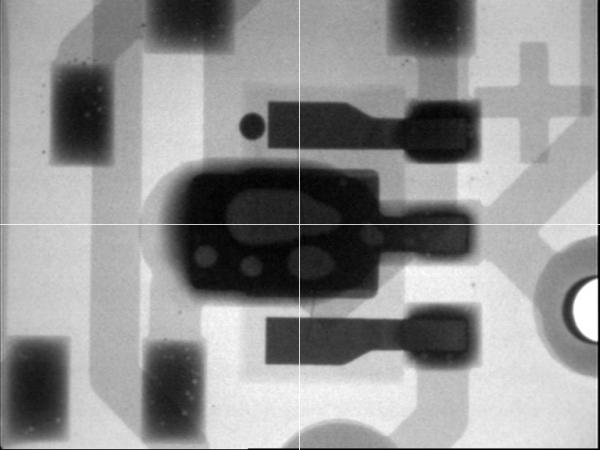
X-ray inspections help us to perform fast and sophisticated optical X-ray inspection of assembled printed circuit boards. The X-ray method is mainly used where automatic optical inspection (AOI) reaches its limits: for highly integrated assemblies with very small distances, for assembled PCBs where the solder joints are not optically visible due to masking (Ball Grid Array, BGA) as well as multilayer PCBs where tracks to be inspected remain hidden for AOI.
Functional test (FT):
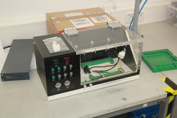
Functional tests (FT) are used to test the concrete, correct functionality of electronic modules, devices and systems. Peripheral tests can also be included in these tests.
Compared to other test procedures, however, the depth of testing is to be considered rather small, which is why functional tests are often used in combination with other test procedures.
Functional tests require the use of special test systems, which we develop for you according to your specific requirements - or use test systems provided by our customers.
Mechanical wear and stress tests:
To comprehensively test the durability of mechanical components and assemblies, we develop individual wear and stress tests that allow us to assess the effect of forces as well as ageing and wear phenomena as a function of a simulated service life in terms of usability and robustness.
Sampling, periodic sampling, routine tests
In our quality control we always test at least on the basis of a random sample from the respective production batch. The size of the random sample depends, among other things, on the size of the batch itself. Depending on the requirements and agreement with the customer, we also carry out periodic tests, whereby we coordinate and agree test and cycle times individually. If required, we also carry out routine tests (i.e. each individual product).
Traceability:
Traceability is of great importance in the context of product safety in electronics production. If a component is found to be defective after production despite all probability, traceability makes it possible to trace the use of the component concerned down to each individual assembly. In order to make this possible, we at AMS rely on comprehensive labeling - and have equipped all our automatic placement machines with probably the most advanced label feeders of their kind: the Automatic Label Feeders of our ALF product lines. //ALF
Related content
Quality - Our certifications and memberships
Hier können Sie sich unsere Zertifikate ansehen und herunterladen.


